Metal-oxide-semiconductor field-effect transistor
The Metal-oxide-semiconductor field-effect transistor (MOSFET) is a type of FET that consists of three layers: a metal top electrode (a conductor, called the gate), an oxide layer (working as an insulator separating the gate from the semiconductor layer), and a semiconductor layer (called the body). Its operation is based upon the modulation of the semiconductor conductivity by the electric field introduced in the body by the gate, the so-called field effect. This transistor was invented by Dawon Khang and Martin Atalla in 1960, at Bell Labs.[1]
There are four contacts altogether: in addition to the gate and body contacts already described, there are two contacts atop the body at opposite sides of the gate called source and drain. Because the transistor is symmetrical, they can swap their functions. They do not permit current flow to the body in normal operation, as they form reverse biased diodes with the body. They do allow current between source and drain upon formation (by the gate) of a surface channel at the top surface of the body, next to the insulator. The channel conductivity depends upon the voltage difference between the gate and body (Vgb). The amount of current drawn in the channel depends upon the voltage drop across it, the drain to source voltage (Vds). The channel strength also is affected by so-called "back gate bias", that is, by the body to source voltage (Vbs).
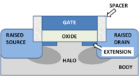
The modern MOSFET structure is shown in the figure (with a bow to artistic license). It is rather complex, as it is made to control a number of undesirable or parasitic effects that detract from its ideal behavior. Among these are unwanted capacitances between the gate and source and gate and drain, reduced by introduction of spacers at the sides of the gate. Another problem is high source-to-body and drain-to-body capacitance, which is reduced by raising the source and drain above the body, so the sidewall contact areas are reduced. These parasitic capacitances have to be charged and discharged between on and off conditions, and slow down device operation. Also undesired is penetration of the source and drain fields underneath the gate, which interferes with the channel formation. That effect is reduced by use of shallow junction extensions and screening halo implants, both designed to keep the source and drain fields close to their electrodes, and away from the gate.
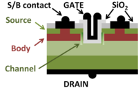
For power applications a different geometry is used, notably asymmetric in drain and source geometry. Special attention is given to the drain, which is adapted to large drain voltages. The figure shows an example called the UMOSFET because of the U-shaped gate. This cross-section is only one from a huge array of identical parallel fingers (the diagram is repeated to right and left with identical structures) all tied together in one device to handle large currents.[2] As indicated by different colors in the figure, the source and drain are both n-type, and the body is p-type, or vice versa. The drain is specially doped to have a wide drift region, allowing reduction of the large drain voltage before it reaches the channel, and also allowing the current from the channel to spread out before reaching the drain contact, lowering the device resistance. The channel is present only when the gate voltage is large enough to turn the device "on", forming an inversion layer.
History
Modern electronic circuits use the MOSFET.
In 1930, Julius Edgar Lilienfeld (1881-1963), from the University of Leipzig applied for a patent in which he described an element bearing resemblance to the MOS transistor and which could have been the first transistor in history. We had to wait until the 1960s in order to see the arrival of such devices, whose development was made possible with the resolution of many technical issues outlined below. Today, the MOS transistor is the key element of digital integrated circuits on a large scale. Despite the origination at Bell Labs of many of the key patents for devices and processes underlying integrated circuits, including the MOSFET, the parent company AT&T never capitalized upon this research to become a big player in this industry, today perhaps the most complex and sophisticated manufacturing enterprise on the planet.
A major obstacle that had to be overcome in realizing this device was the quality of the semiconductor-insulator interface, which in many materials systems contains a large number of interface traps that interfere with the field effect. It was found that the interface between silicon and silicon dioxide was close to ideal in this respect if care was taken in its preparation (a technique called surface passivation). A stability issue required removal of mobile ion contaminants from the oxide, notably sodium, which required careful control of all fabrication steps, and today is accomplished in manufacturing by controlled atmosphere clean rooms that keep all contaminants to very low levels never envisioned prior to manufacture of this device.[3] A major source of contaminants is the human body, so a modern "fab" requires operators to wear specially constructed bunny suits, with "booties", gowns, gloves, hair caps and masks.[4] A modern fabrication center costs about one to ten billion US dollars, with a very hefty operational budget.[5][6]
More recently, the challenges for MOSFET design are related to its miniaturization. Miniaturization of the transistor cannot be separated from the evolution of the entire circuit, as the layout of devices and circuits are combined in the same steps. A modern integrated circuit uses perhaps more than a billion of these devices[7] with dimensions in the range of tens of nm.[8] Miniaturization has required entirely new fabrication methods, such as ion implantation to control dopant locations very accurately, sophisticated self-aligned masking steps to construct tiny geometries,[9] and development of chemical procedures and metallurgy with rigid thermal budgets. This package of processes is sometimes called silicon planar technology.[10] The complexity of this processing and of circuits with millions of devices has led to development of computer-aided design involving sophisticated software that simulates everything from individual processes and devices to the layout of the entire circuit and the precise simulation of each step in its manufacture. Expense places a premium upon "right-the-first-time" manufacture: the concepts of electronic design automation and design for manufacture are applied with mind-boggling rigor.[11]
Operation
A narrow, surface inversion layer of electrons forms at large enough positive gate voltages. The horizontal dashed line indicates the Fermi level, the energy of levels (should they exist) that are half-occupied at the selected temperature.
The control of the channel by the gate is similar to the formation of an inversion layer in the MOS capacitor, which is only a two-terminal device (gate and body contacts). The case of a p-type semiconductor body in which mobile holes are introduced in the valence band by introducing acceptor impurities is described below. The acceptors suck electrons out of the valence band, becoming fixed negative ions, and leaving electron vacancies in the valence band that behave as positively charge mobile holes.
The formation of this layer is understood by examining the behavior of the energy band edges under an applied field. The left-hand panels of the figure depict the lowest energy level of the conduction band of energies and the highest energy level of the valence band of energies (separated by the forbidden gap with no available energy levels) as a function of depth into the semiconductor body. In the figure's top panel, an applied voltage bends these band edges (left). This bending causes the valence band to become filled with electrons, so no holes are present. On the upper right, the figure shows the charge inducing this bending (Q) is balanced by a layer of negative acceptor-ion charge –QA in this depletion region where there are no holes. This depletion region of negative acceptor ions widens until neutrality is reached Q−QA = 0. In the bottom panel, a larger applied voltage further depletes holes from the surface but the conduction band becomes low enough in energy to populate with electrons near the surface, forming an inversion layer. The charge inducing the inversion layer is now balanced both by the inversion layer charge –Qn and by the depletion layer charge –QA, so now Q–Qn−QA = 0. Once the applied voltage is large enough to begin formation of the inversion layer, the charge balance is dominated by this layer, and the depletion region no longer expands significantly.
The electrons in the surface channel are mobile and form a conducting surface layer atop the insulating layer of fixed, immobile acceptor ions in the depletion region. The source and drain contacts on the body surface become connected by this conducting surface layer, so the formation of the inversion layer allows current to flow from the source to the drain. By contrast, when the conducting surface layer is not present, no conduction occurs, even when the surface layer is not depleted and holes are present. The contacts cannot conduct using holes because they are n-type semiconductor regions, and form pn-diode junctions with the body.
Thus, the source and drain are not electrically connected for voltages between zero and the threshold voltage for inversion layer formation. But once threshold voltage is exceeded, connection is established. The MOSFET constitutes an electrically controlled switch. The quantitative current-voltage behavior of the modern MOSFET is described by complex computer models.[12]
Two device types: n- and p-channel
The device above uses a p-type body and an electron inversion layer, or n-channel. In CMOS circuits these n-channel MOSFETs are combined with p-channel MOSFETs that use an n-type body and a hole inversion layer. These CMOS circuits consume low power as only the active devices in a sub-circuit (either the n-channel or the p-channel devices) are operational at a given time, and the complementary devices are "off".
Frequency dependence
See also MOSFET hybrid pi model
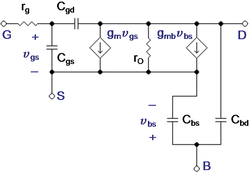
An important device quality is its speed of response to transient signals. The MOSFET is a very non-linear device, so its transient response for large signals requires a numerical calculation. However, some idea is gained using a small-signal model and treating the device for small variations about a quiescent condition (its Q-point). Such a circuit is shown in the figure for a device biased in active mode. This circuit reduces the problem of frequency response to the RC time-constants related to charge and discharge of various capacitances through their associated resistors.
Four terminals are shown, the gate G, the source S, the drain D and the body B.
In many circuits the source terminal is short-circuited to the body terminal so voltage vbs = 0 V. Then the circuit elements with b in the subscript can be ignored with the exception of Cbd, and the circuit becomes a version of the hybrid-pi model for the bipolar transistor with an infinite rπ resistance and an input capacitance Cgs similar to the Cπ capacitance of the bipolar, but with no diffusion capacitance contribution. However, even with the body short-circuited to the drain, the capacitance Cbd is present as, in effect, a load capacitance upon the circuit. It should not be neglected, although many textbook discussions leave it out to keep things simpler.
A peculiarity of the MOSFET capacitances is the treatment of the channel. Commonly the capacitance Cgd includes coupling between the gate and the drain-end of the channel, while Cgs couples to the source-end of the channel. This matter can be decided with a full blown microscopic numerical analysis, but for circuit design faster modeling is needed. In these models, uncertainty over how this contribution is divided (that is, how much of the channel goes to the source-end capacitance and how much to the drain-end) leads to some slop in predicting the behavior of this device at frequencies above the corner frequency. If all the channel is attached to the source, the device is slower than when half goes to the source and half to the drain, for example. Arbitrarily, this ratio commonly is set at 60% source/40% drain. [13]
Output resistance
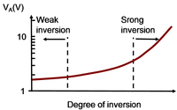
Early voltage for MOSFETs from a 0.18μm process as a function of inversion level (channel strength). These are measured values with VDS = VGS.[14]
In analog applications such as current mirrors or active loads, it is important for the transistor to have a large output resistance. Such circuits emulate a current source or current sink, and the Norton resistance of such a circuit should be large for ideal behavior.
The output resistance, usually denoted by rO, is a measure of how much drain-to-source voltage change is necessary to cause a given change in transistor output current when the transistor is in active mode. This resistance depends upon VGS, of course, because the channel conductivity depends upon the number of carriers within it, and that increases with gate voltage. However, rO also varies with VDS.
The reason a change in drain bias changes the resistance is that the channel exists only when the oxide field is sufficient to form a channel. At the source itself the oxide field is dependent upon the voltage drop VGS, which in active mode is above the threshold voltage, and so a channel forms. However, near the drain the oxide field depends upon VGD, and the applied drain voltage VDS makes VGD smaller than VGS because VDS brings the drain closer in voltage to the gate than is the source. The field in the oxide above the channel interpolates between these two values. In the ohmic or triode mode, a channel exists all the way from source to drain. But in the active mode, the drain voltage is high enough that somewhere between the source and drain the oxide field becomes too low to form a channel. The channel ends and dumps its carriers into the bulk semiconductor to finish their trip toward the drain without a channel. The termination of the channel is called the pinch-off point and it moves toward the source as the drain voltage increases. The channel becoming shorter as drain bias increases, the resistance between source and pinch-off point drops, so there results a lowering of output resistance with increase in drain bias. This phenomenon is called either channel-length modulation or the Early effect.
According to a simple empirical model patterned after the bipolar model for output resistance, the output resistance is given by:
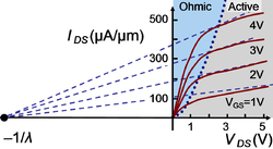
where λ is called the channel-length modulation parameter with dimensions V−1 and 1/λ plays the role of the Early voltage VA found in the bipolar model. The current IDS(VGS, VDS) is the drain current evaluated at the selected gate and drain voltages. It should be noted that this formula for output resistance is largely a fiction of hand analysis, and cannot be trusted. For example, the figure shows a tentative attempt to establish λ for a rather old 3/4μm technology. A single value for λ provides only a crude indicator of the slope of these curves in active mode.
To illustrate that λ is a function, not a constant, the lower figure shows measured values of VA=1/λ for a 0.18μm MOSFET process at a bias in the active mode of VGD=VGS−VDS=0 V. Here, VA = 1/λ increases by an order of magnitude as the channel becomes stronger. The need to employ a variety of λ-values is even greater in today's technology where λ is a function of device geometry in three dimensions (not just channel length, although this is important) and bias voltages. In practice, a particular value is calculated for each situation using a numerical model of the transistor or is measured directly.
Generally speaking, the output resistance of MOSFETs is low, and where high resistance is necessary, special circuit techniques involving multiple transistors are implemented to increase the effective resistance.
Shichman-Hodges model
For hand analysis of circuit design the DC current voltage behavior of the MOSFET in active mode often is discussed using the Shichman-Hodges model. The drain current is given by:
with W, L the width and "effective" length of the device, VT the threshold voltage, and λ the channel-length modulation factor. The "technology parameter" k’n is estimated from an empirical value for the carrier mobility in the channel and the oxide capacitance: k’n = μeffCOX. Simply because some model is necessary for hand analysis to guide design prior to committing to numerical simulation, great effort has been wasted to invest this model with an accuracy that remains beyond its capabilities, no matter how convoluted the use of "effective" parameters. Aside from parameters with implicit bias and geometry dependence that is not spelled out, especially λ, the quadratic dependence upon gate-to-source voltage is not observed in modern MOSFETs, with the exception of some specialized structures like power MOSFETs.
For example, in the above figure, the IV-curves show a linear dependence upon gate voltage, primarily due to a decrease in mobility of the carriers at large electric fields called velocity saturation. In a situation where the velocity of the carriers becomes independent of the electric field along the channel, the current depends upon only the carrier density and the saturated velocity, and as the carrier density is set by the oxide field according to Gauss' law as proportional to VGS, a linear dependence of current upon VGS results.
Because of the limitations of algebraic models, modern hand analysis of circuit design has become an amalgam of numeric and algebraic methods.
Notes
- ↑ An historical run-down with references can be found in Gianfranco Cerofolini (2009). “Chapter 2: Top-down paradigm to miniaturization”, Nanoscale Devices: Fabrication, Functionalization, and Accessibility from the Macroscopic World. Springer, pp. 9 ff. ISBN 354092731X.
- ↑ B. Jayant Baliga (2010). “Chapter 3: U-MOSFET structure”, Advanced Power MOSFET Concepts. Springer, p. 66 ff. ISBN 1441959165.
- ↑ For a discussion, see Peter Van Zant (2004). “Chapter 5: Contamination control”, Microchip fabrication: a practical guide to semiconductor processing, 5th ed. McGraw-Hill, pp. 91 ff. ISBN 0071432418.
- ↑ See previously cited work Peter Van Zant. Microchip fabrication: a practical guide to semiconductor processing, pp. 112. ISBN 0071432418.
- ↑ Intel breaks ground in China for US $2.5 billion silicon fabrication plant. The China Post (2007). Retrieved on 2011-01-23.
- ↑ July 16, 2010 Taiwan Semiconductor Manufacturing Corporation (TSMC) announced its third GigafabTM expected to cost more than NT$300 billion ≈ $10 billion USD. See TSMC begins construction on GigafabTM in central Taiwan. News Archives/Business. TSMC (2010-07-16). Retrieved on 2011-03-16.
- ↑ For example, see Jon Stokes (2/9/2010). Two billion-transistor beasts: POWER7 and Niagara 3. ars technica. Retrieved on 2011-01-23.
- ↑ A rule of thumb much used in the industry is Moore's law, which predicts a 20nm design rule will be realized in 2011. Already in mid-2010 initial fabrication had begun on the 22nm design node. See TSMC skips 22 nm, rolls 20-nm process. EE Times (4/13/2010). Retrieved on 2011-01-16.
- ↑ The techniques of microlithography involve a variety of masks and radiations that expose patterns that are then etched or "developed". See for example, J. Michael Köhler, Wolfgang Fritzsche (2007). “§3.4 Structure generation and fabrication of lithographic masks”, Nanotechnology: an introduction to nanostructuring techniques, 2nd ed. Wiley-VCH, p. 59. ISBN 3527318712.
- ↑ For a discussion, see for example, Chue San Yoo (2008). “§1.2 Evolution of integrated circuit industry”, Semiconductor manufacturing technology. World Scientific, pp. 5 ff. ISBN 9812568239.
- ↑ A selection of essays on these topics is found in (2006) Louis Scheffer, ed.: Electronic design automation for integrated circuits handbook, Volume 2. CRC Press. ISBN 0849379237. An historical review is found in Laung-Terng Wang, Yao-Wen Chang, Kwang-Ting Cheng (2009). “§1.1.1 Historical perspective”, Electronic design automation: synthesis, verification, and test. Morgan Kaufmann, pp. 2 ff. ISBN 0123743648.
- ↑ A popular MOSFET computer model is BSIM4, see: BSIM4.6.4 MOSFET Model: User's manual. BSIM 4 web site. Electrical Engineering and Computer Sciences Department, UC Berkeley (2009). Retrieved on 2011-05-20. This 170-page manual describes a model much more complex than a simple algebraic formula.
- ↑ JR Brews (January/February, 2006). "MOSFET hand analysis using BSIM". IEEE Circuits and Devices 22 (1): pp. 28 ff. DOI:10.1109/MCD.2006.1598077. Research Blogging.
- ↑ Patterned after Figure 3.49, p. 159 in David Binkley (2008). Tradeoffs and Optimization in Analog CMOS Design. Wiley-Interscience. ISBN 0470031360.
