imported>John R. Brews |
imported>John R. Brews |
| Line 1: |
Line 1: |
| {{TOC|right}} | | {{TOC|right}} |
| A '''current mirror''' is a circuit designed to copy a [[current (electricity)|current]] through one [[active device]] by controlling the current in another active device of a circuit, keeping the output current constant regardless of loading. The current being 'copied' can be, and sometimes is, a varying signal current. Conceptually, an ideal current mirror is simply an ideal current amplifier. The current mirror is used to provide bias currents and [[active load]]s to circuits.
| |
|
| |
|
| ==Mirror characteristics== | | [[Image:Two-port parameters.PNG|thumb|180px|right|Figure 1: Example two-port network with symbol definitions. Notice the '''port condition''' is satisfied: the same current flows into each port as leaves that port.]] |
| There are three main specifications that characterize a current mirror. The first is the current level it produces. The second is its AC output resistance, which determines how much the output current varies with the voltage applied to the mirror. The third specification is the minimum voltage drop across the mirror necessary to make it work properly. This minimum voltage is dictated by the need to keep the output transistor of the mirror in active mode. The range of voltages where the mirror works is called the '''compliance range''' and the voltage marking the boundary between good and bad behavior is called the '''compliance voltage'''. There are also a number of secondary performance issues with mirrors, for example, temperature stability.
| | A '''Two Port Network''' (or '''four-terminal network''', or '''quadrapole''') is an [[electrical circuit]] or device with two ''pairs'' of terminals. Two terminals constitute a '''port''' if they satisfy the essential requirement known as the '''port condition''': the same current must enter and leave a port.<ref name=Gray> |
| | {{cite book |
| | |author=P.R. Gray, P.J. Hurst, S.H. Lewis, and R.G. Meyer |
| | |title=Analysis and Design of Analog Integrated Circuits |
| | |year= 2001 |
| | |edition=Fourth Edition |
| | |publisher=Wiley |
| | |location=New York |
| | |isbn=0471321680 |
| | |pages=§3.2, p. 172 |
| | |url=http://worldcat.org/isbn/0471321680}} |
| | </ref><ref name=Jaeger> |
| | {{cite book |
| | |author=R. C. Jaeger and T. N. Blalock |
| | |title=Microelectronic Circuit Design |
| | |year= 2006 |
| | |edition=Third Edition |
| | |publisher=McGraw-Hill |
| | |location=Boston |
| | |isbn=9780073191638 |
| | |pages=§10.5 §13.5 §13.8 |
| | |url=http://worldcat.org/isbn/9780073191638}} |
| | </ref> |
| | Examples include small-signal models for transistors (such as the [[hybrid-pi model]]), [[electronic filter|filter]]s and [[matching network]]s. The analysis of passive two-port networks is an outgrowth of reciprocity theorems first derived by Lorentz. See review by [http://www.ieee.org/organizations/pubs/newsletters/emcs/summer03/jasper.pdf Jasper J. Goedbloed, ''Reciprocity and EMC measurements''. ] |
| | |
| | A two-port network makes possible the isolation of either a complete circuit or part of it and replacing it by its characteristic parameters. Once this is done, the isolated part of the circuit becomes a "[[black box]]" with a set of distinctive properties, enabling us to abstract away its specific physical buildup, thus simplifying analysis. Any linear circuit with four terminals can be transformed into a two-port network provided that it does not contain an independent source and satisfies the port conditions. |
| | |
| | The parameters used in order to describe a two-port network are the following: z, y, h, g, T. They are usually expressed in matrix notation and they establish relations between the following parameters (see Figure 1): |
| | :<math>{V_1}</math> = Input voltage |
| | :<math>{V_2}</math> = Output voltage |
| | :<math>{I_1}</math> = Input current |
| | :<math>{I_2}</math> = Output current |
| | These variables are most useful at low to moderate frequencies. At high frequencies (for example, microwave frequencies) power and energy are more useful variables, and the two-port approach based on current and voltages that is discussed here is replaced by an approach based upon [[scattering parameters]]. |
| | |
| | Though some authors use the terms ''two-port network'' and ''four-terminal network'' interchangeably, the latter represents a more general concept. '''Not all four-terminal networks are two-port networks.''' A pair of terminals can be called a ''port'' only if the current entering one is equal to the current leaving the other (the '''port condition'''). Only those four-terminal networks in which the four terminals can be paired into two ports can be called two-ports.<ref name=Gray> |
| | {{cite book |
| | |author=P.R. Gray, P.J. Hurst, S.H. Lewis, and R.G. Meyer |
| | |title=Analysis and Design of Analog Integrated Circuits |
| | |year= 2001 |
| | |edition=Fourth Edition |
| | |publisher=Wiley |
| | |location=New York |
| | |isbn=0471321680 |
| | |pages=§3.2, p. 172 |
| | |url=http://worldcat.org/isbn/0471321680}} |
| | </ref><ref name=Jaeger> |
| | {{cite book |
| | |author=R. C. Jaeger and T. N. Blalock |
| | |title=Microelectronic Circuit Design |
| | |year= 2006 |
| | |edition=Third Edition |
| | |publisher=McGraw-Hill |
| | |location=Boston |
| | |isbn=9780073191638 |
| | |pages=§10.5 §13.5 §13.8 |
| | |url=http://worldcat.org/isbn/9780073191638}} |
| | </ref> |
|
| |
|
| ==Practical approximations== | | == Impedance parameters (z-parameters)== |
| For small-signal analysis the current mirror can be approximated by its equivalent [[Norton's theorem| Norton impedance]] .
| | [[Image:Z-equivalent two port.png|thumbnail|300px| Figure 2: z-equivalent two port showing independent variables ''I<sub>1</sub>'' and ''I<sub>2</sub>''. Although resistors are shown, general impedances can be used instead.]] |
| | {{main|Impedance parameters}} |
|
| |
|
| In large-signal hand analysis, a current mirror usually is approximated simply by an ideal current source. However, an ideal current source is unrealistic in several respects:
| | :<math> \left[ \begin{array}{c} V_1 \\ V_2 \end{array} \right] = \left[ \begin{array}{cc} z_{11} & z_{12} \\ z_{21} & z_{22} \end{array} \right] \left[ \begin{array}{c}I_1 \\ I_2 \end{array} \right] </math>. |
| *it has infinite AC impedance, while a practical mirror has finite impedance
| |
| *it provides the same current regardless of voltage, that is, there are no compliance range requirements
| |
| *it has no frequency limitations, while a real mirror has limitations due to the parasitic capacitances of the transistors
| |
| *the ideal source has no sensitivity to real-world effects like noise, power-supply voltage variations and component tolerances.
| |
|
| |
|
| == Circuit realizations of current mirrors == | | :<math>z_{11} = {V_1 \over I_1 } \bigg|_{I_2 = 0} \qquad z_{12} = {V_1 \over I_2 } \bigg|_{I_1 = 0}</math> |
| {{Image|Simple bipolar mirror.PNG|right|250px|A current mirror implemented with npn bipolar transistors using a resistor to set the reference current I<sub>REF</sub>; V<sub>CC</sub> = supply voltage.}} | |
|
| |
|
| ===Basic bipolar transistor mirror=== | | :<math>z_{21} = {V_2 \over I_1 } \bigg|_{I_2 = 0} \qquad z_{22} = {V_2 \over I_2 } \bigg|_{I_1 = 0}</math> |
| The simplest bipolar current mirror consists of two transistors connected as shown in the figure. Transistor Q<sub>1</sub> is connected so its collector-base voltage is zero. Consequently, the voltage drop across Q<sub>1</sub> is ''V''<sub>BE</sub>, that is, this voltage is set by the [[Diode_modelling#Shockley_diode_model| diode law]] and Q<sub>1</sub> is said to be '''diode connected'''. (See also [[Bipolar_transistor#Ebers.E2.80.93Moll_model|Ebers-Moll model]].) It is important to have Q<sub>1</sub> in the circuit instead of a simple diode, because Q<sub>1</sub> sets ''V<sub>BE</sub>'' for the transistor Q<sub>2</sub>. If Q<sub>1</sub> and Q<sub>2</sub> are matched, that is, have substantially the same device properties, and if the mirror output voltage is chosen so the collector-base voltage of Q<sub>2</sub> also is zero, then the ''V<sub>BE</sub>''-value set by Q<sub>1</sub> results in an emitter current in the matched Q<sub>2</sub> that is the same as the emitter current in Q<sub>1</sub>. Because Q<sub>1</sub> and Q<sub>2</sub> are matched, their β<sub>0</sub>-values also agree, making the mirror output current the same as the collector current of Q<sub>1</sub>.
| |
| The current delivered by the mirror for arbitrary collector-base reverse bias ''V''<sub>CB</sub> of the output transistor is given by (see [[bipolar transistor]]):
| |
|
| |
|
| ::<math> I_\mathrm{C} = I_\mathrm{S} \left( e^{\frac{V_\mathrm{BE}}{V_\mathrm{T}}}-1 \right) \left(1 + \begin{matrix} \frac{V_\mathrm{CB}}{V_\mathrm{A}} \end{matrix} \right) </math>,
| | Notice that all the z-parameters have dimensions of ohms. |
| where ''V<sub>T</sub>'' = [[Boltzmann constant#Role in semiconductor physics: the thermal voltage|thermal voltage]], ''I<sub>S</sub>'' = reverse saturation current, or scale current; ''V<sub>A</sub>'' = [[Early voltage]]. This current is related to the reference current ''I<sub>REF</sub>'' when the output transistor ''V<sub>CB</sub>'' = 0 V by:
| |
|
| |
|
| ::<math> I_{REF} = I_C \left( 1+ \frac {2} {\beta_0} \right) \ , </math> | | ===Example: bipolar [[current mirror]] with emitter degeneration=== |
| | [[Image:Current mirror.png|thumbnail|left|200px| Figure 3: Bipolar current mirror: ''i<sub>1</sub>'' is the ''reference current'' and ''i<sub>2</sub>'' is the ''output current''; lower case symbols indicate these are ''total'' currents that include the DC components]] |
| | [[Image:Smal-signal mirror circuit.png|thumbnail|right|300px| Figure 4: Small-signal bipolar current mirror: ''I<sub>1</sub>'' is the amplitude of the small-signal ''reference current'' and ''I<sub>2</sub>'' is the amplitude of the small-signal ''output current'']] |
| | Figure 3 shows a bipolar current mirror with emitter resistors to increase its output resistance.<ref>The emitter-leg resistors counteract any current increase by decreasing the transistor ''V<sub>BE</sub>''. That is, the resistors ''R<sub>E</sub>'' cause negative feedback that opposes change in current. In particular, any change in output voltage results in less change in current than without this feedback, which means the output resistance of the mirror has increased.</ref> Transistor ''Q<sub>1</sub>'' is ''diode connected'', which is to say its collector-base voltage is zero. Figure 4 shows the small-signal circuit equivalent to Figure 3. Transistor ''Q<sub>1</sub>'' is represented by its emitter resistance ''r<sub>E</sub>'' ≈ ''V<sub>T</sub> / I<sub>E</sub>'' (''V<sub>T</sub>'' = thermal voltage, ''I<sub>E</sub>'' = [[Q-point]] emitter current), a simplification made possible because the dependent current source in the hybrid-pi model for ''Q<sub>1</sub>'' draws the same current as a resistor 1 / ''g<sub>m</sub>'' connected across ''r<sub>π</sub>''. The second transistor ''Q<sub>2</sub>'' is represented by its [[hybrid-pi model]]. Table 1 below shows the z-parameter expressions that make the z-equivalent circuit of Figure 2 electrically equivalent to the small-signal circuit of Figure 4. |
| | {| class="wikitable" style="background:white;text-align:center;margin: 1em auto 1em auto" |
| | !Table 1 !! Expression !! Approximation |
|
| |
|
| as found using [[Kirchhoff's current law]] at the collector node of Q<sub>1</sub>. The reference current supplies the collector current to Q<sub>1</sub> and the base currents to both transistors — when both transistors have zero base-collector bias, the two base currents are equal. Parameter β<sub>0</sub> is the transistor β-value for ''V''<sub>CB</sub> = 0 V.
| | |-valign="center" |
| | |<math>R_{21} = \begin{matrix} {V_\mathrm{2} \over I_\mathrm{1} }\end{matrix} \Big|_{I_{2}=0} </math> |
| | |<math> - ( \beta r_O - R_E ) </math> <math> \begin{matrix} \frac {r_E +R_E }{r_{ \pi}+r_E +2R_E} \end{matrix} </math> |
| | |<math> - \beta r_o </math><math> \begin{matrix} \frac {r_E+R_E }{r_{ \pi} +2R_E}\end{matrix} </math> |
|
| |
|
| ====Output resistance==== | | |-valign="center" |
| If V<sub>CB</sub> is greater than zero in output transistor Q<sub>2</sub>, the collector current in Q<sub>2</sub> will be somewhat larger than for Q<sub>1</sub> due to the [[Early effect]]. In other words, the mirror has a finite output (or Norton) resistance given by the ''r<sub>O</sub>'' of the output transistor, namely (see [[Early effect]]):
| | |<math>R_{11}= \begin{matrix} \frac{V_{1}}{I_{1}}\end{matrix} \Big|_{I_{2}=0} </math> |
| | |<math> (r_E + R_E)</math> <math>// </math> <math>(r_{ \pi} +R_E) </math> |
| | |<math></math> |
|
| |
|
| ::<math> R_N =r_O = \begin{matrix} \frac {V_A + V_{CB}} {I_C} \end{matrix} </math>,
| | |-valign="center" |
| | |<math> R_{22} = \begin{matrix} \frac{V_{2}}{I_{2}}\end{matrix} \Big|_{I_{1}=0} </math> |
| | |<math> \ ( </math><math> 1 + \beta </math> <math> \begin{matrix} \frac {R_E} {r_{ \pi} +r_E+2R_E } \end{matrix} ) </math> <math> r_O </math> <math>+ \begin{matrix} \frac { r_{ \pi}+r_E +R_E }{r_{ \pi}+r_E +2R_E } \end{matrix} </math><math>R_E</math> |
| | |<math> \ ( </math><math>1 + \beta </math><math> \begin{matrix} \frac {R_E} {r_{ \pi}+2R_E } \end{matrix} ) </math> <math>r_O </math> |
|
| |
|
| where ''V<sub>A</sub>'' = Early voltage and ''V<sub>CB</sub>'' = collector-to-base bias.
| | |-valign="center" |
| ====Compliance voltage====
| | |<math> R_{12} = \begin{matrix} {V_\mathrm{1} \over I_\mathrm{2} }\end{matrix} \Big|_{I_{1}=0} </math> |
| To keep the output transistor active, ''V<sub>CB</sub>'' ≥ 0 V. That means the lowest output voltage that results in correct mirror behavior, the compliance voltage, is ''V<sub>OUT</sub>'' = ''V<sub>CV</sub>'' = ''V<sub>BE</sub>'' under bias conditions with the output transistor at the output current level ''I<sub>C</sub>'' and with ''V<sub>CB</sub>'' = 0 V or, inverting the ''I-V'' relation above:
| | |<math>R_E </math> <math>\begin{matrix} \frac {r_E+R_E} {r_{ \pi} +r_E +2R_E} \end{matrix}</math> |
| | |<math>R_E</math> <math> \begin{matrix} \frac {r_E+R_E} {r_{ \pi} +2R_E} \end{matrix}</math> |
| | |} |
|
| |
|
| ::<math>\ V_{CV}= {V_T}</math> <math>\ \mathrm {ln} </math> <math> \left(\begin{matrix}\frac {I_C}{I_S}\end{matrix}+1\right) \ , </math>
| | The negative feedback introduced by resistors ''R<sub>E</sub>'' can be seen in these parameters. For example, when used as an active load in a differential amplifier, ''I<sub>1</sub> ≈ -I<sub>2</sub>'', making the output impedance of the mirror approximately ''R<sub>22</sub> -R<sub>21</sub>'' ≈ 2 β ''r<sub>O</sub>R<sub>E</sub>'' /( ''r<sub>π</sub>+2R<sub>E</sub>'' ) compared to only ''r<sub>O</sub>'' without feedback (that is with ''R<sub>E</sub>'' = 0 Ω) . At the same time, the impedance on the reference side of the mirror is approximately ''R<sub>11</sub> -R<sub>12</sub>'' ≈ <math> \begin{matrix} \frac {r_{\pi}} {r_{\pi}+2R_E} \end{matrix} </math> <math> (r_E+R_E)</math>, only a moderate value, but still larger than ''r<sub>E</sub>'' with no feedback. In the differential amplifier application, a large output resistance increases the difference-mode gain, a good thing, and a small mirror input resistance is desirable to avoid [[Miller effect]]. |
|
| |
|
| where ''V<sub>T</sub>'' = [[Boltzmann constant#Role in semiconductor physics: the thermal voltage|thermal voltage]] and ''I<sub>S</sub>'' = reverse saturation current (scale current).
| | ==Admittance parameters (y-parameters) == |
| | [[Image:Y-parameter two-port.PNG|thumbnail|300px| Figure 5: Y-equivalent two port showing independent variables ''V<sub>1</sub>'' and ''V<sub>2</sub>''. Although resistors are shown, general admittances can be used instead.]] |
| | {{main|Admittance parameters}} |
|
| |
|
| ====Extensions and complications====
| | :<math> \left[ \begin{array}{c} I_1 \\ I_2 \end{array} \right] = \left[ \begin{array}{cc} y_{11} & y_{12} \\ y_{21} & y_{22} \end{array} \right] \left[ \begin{array}{c}V_1 \\ V_2 \end{array} \right] </math>. |
| When Q<sub>2</sub> has ''V<sub>CB</sub>'' > 0 V, the transistors no longer are matched. In particular, their β-values differ due to the Early effect, with
| |
| ::<math>{\beta}_1 = {\beta}_{0} \ \operatorname{and} \ {\beta}_2 = {\beta}_{0}\ (1 + \frac{V_{CB}}{V_A})</math>
| |
| where V<sub>A</sub> is the [[Early effect|Early voltage]] and β<sub>0</sub> = transistor β for V<sub>CB</sub> = 0 V. Besides the difference due to the Early effect, the transistor β-values will differ because the β<sub>0</sub>-values depend on current, and the two transistors now carry different currents (see [[Gummel–Poon model|Gummel-Poon model]]).
| |
|
| |
|
| Further, Q<sub>2</sub> may get substantially hotter than Q<sub>1</sub> due to the associated higher power dissipation. To maintain matching, the temperature of the transistors must be nearly the same. In [[integrated circuit]]s and transistor arrays where both transistors are on the same die, this is easy to achieve. But if the two transistors are widely separated, the precision of the current mirror is compromised.
| | where |
|
| |
|
| Additional matched transistors can be connected to the same base and will supply the same collector current. In other words, the right half of the circuit can be duplicated several times with various resistor values replacing R<sub>2</sub> on each. Note, however, that each additional right-half transistor "steals" a bit of collector current from Q<sub>1</sub> due to the non-zero base currents of the right-half transistors. This will result in a small reduction in the programmed current.
| | :<math>y_{11} = {I_1 \over V_1 } \bigg|_{V_2 = 0} \qquad y_{12} = {I_1 \over V_2 } \bigg|_{V_1 = 0}</math> |
|
| |
|
| An example of a mirror with emitter degeneration to increase mirror resistance is found in [[Two-port network#Impedance parameters (z-parameters)|two-port network]]s.
| | :<math>y_{21} = {I_2 \over V_1 } \bigg|_{V_2 = 0} \qquad y_{22} = {I_2 \over V_2 } \bigg|_{V_1 = 0}</math> |
|
| |
|
| For the simple mirror shown in the diagram, typical values of <math>\beta</math> will yield a current match of 1% or better.
| |
|
| |
|
| === Basic MOSFET current mirror ===
| | The network is said to be reciprocal if <math> y_{12} = y_{21}</math>. Notice that all the Y-parameters have dimensions of siemens. |
| {{Image|Simple MOSFET mirror.PNG|right|250px| An n-channel MOSFET current mirror with a resistor to set the reference current I<sub>REF</sub>; V<sub>DD</sub> is the supply voltage.}}
| |
| The basic current mirror can also be implemented using MOSFET transistors, as shown in the adjacent figure. Transistor ''M''<sub>1</sub> is operating in the [[MOSFET#Modes of operation|saturation or active]] mode, and so is ''M''<sub>2</sub>. In this setup, the output current ''I''<sub>OUT</sub> is directly related to ''I''<sub>REF</sub>, as discussed next.
| |
|
| |
|
| The drain current of a MOSFET ''I''<sub>D</sub> is a function of both the gate-source voltage and the drain-to-gate voltage of the MOSFET given by ''I''<sub>D</sub> = ''f'' (''V''<sub>GS</sub>, ''V''<sub>DG</sub>), a relationship derived from the functionality of the [[MOSFET]] device. In the case of transistor ''M''<sub>1</sub> of the mirror, ''I''<sub>D</sub> = ''I''<sub>REF</sub>. Reference current ''I''<sub>REF</sub> is a known current, and can be provided by a resistor as shown, or by a "threshold-referenced" or "self-biased" current source to insure that it is constant, independent of voltage supply variations.<ref name=Gray-Meyer/>
| | ==Hybrid parameters (h-parameters) == |
| | [[Image:H-equivalent circuit.PNG|thumbnail|300px|Figure 6: H-equivalent two-port showing independent variables ''I<sub>1</sub>'' and ''V<sub>2</sub>''; ''h<sub>22</sub>'' is reciprocated to make a resistor ]] |
| | :<math> {V_1 \choose I_2} = \begin{pmatrix} h_{11} & h_{12} \\ h_{21} & h_{22} \end{pmatrix}{I_1 \choose V_2} </math>. |
|
| |
|
| Using ''V''<sub>DG</sub>=0 for transistor ''M''<sub>1</sub>, the drain current in ''M''<sub>1</sub> is ''I''<sub>D</sub> = ''f'' (''V''<sub>GS</sub>,''V''<sub>DG</sub>=0), so we find: ''f'' (''V''<sub>GS</sub>, 0) = ''I''<sub>REF</sub>, implicitly determining the value of ''V''<sub>GS</sub>. Thus ''I''<sub>REF</sub> sets the value of ''V''<sub>GS</sub>. The circuit in the diagram forces the same ''V''<sub>GS</sub> to apply to transistor ''M''<sub>2</sub>. If ''M''<sub>2</sub> also is biased with zero ''V''<sub>DG</sub> and provided both transistors ''M''<sub>1</sub> and ''M''<sub>2</sub> have good matching of their properties, such as channel length, width, threshold voltage ''etc.'', the relationship ''I''<sub>OUT</sub> = ''f'' (''V''<sub>GS</sub>,''V''<sub>DG</sub>=0 ) applies, thus setting ''I''<sub>OUT</sub> = ''I''<sub>REF</sub>; that is, the output current is the same as the reference current when ''V''<sub>DG</sub>=0 for the output transistor, and both transistors are matched.
| | where |
|
| |
|
| The drain-to-source voltage can be expressed as ''V''<sub>DS</sub>=''V''<sub>DG</sub> +''V''<sub>GS</sub>. With this substitution, the Shichman-Hodges model provides an approximate form for function ''f'' (''V''<sub>GS</sub>,''V''<sub>DG</sub>):<ref name=Gray-Meyer2/>
| | :<math>h_{11} = {V_1 \over I_1 } \bigg|_{V_2 = 0} \qquad h_{12} = {V_1 \over V_2 } \bigg|_{I_1 = 0}</math> |
|
| |
|
| :::<math>
| | :<math>h_{21} = {I_2 \over I_1 } \bigg|_{V_2 = 0} \qquad h_{22} = {I_2 \over V_2 } \bigg|_{I_1 = 0}</math> |
| \begin{alignat}{2}
| |
| I_{d} & = f\ (V_{GS},V_{DG})
| |
| = \begin{matrix} \frac{1}{2}K_{p}\left(\frac{W}{L}\right)\end{matrix}(V_{GS} - V_{th})^2 (1 + \lambda V_{DS}) \\
| |
| & =\begin{matrix} \frac{1}{2}K_{p}\left(\frac{W}{L}\right)\end{matrix}(V_{GS} - V_{th})^2 \left( 1 + \lambda (V_{DG}+V_{GS}) \right) \\
| |
| \end{alignat}</math>
| |
|
| |
|
| where, <math>{K_{p}}</math> is a technology related constant associated with the transistor, ''W/L'' is the width to length ratio of the transistor, ''V''<sub>GS</sub> is the gate-source voltage, ''V''<sub>th</sub> is the threshold voltage, λ is the [[channel length modulation]] constant, and ''V''<sub>DS</sub> is the drain source voltage.
| | Often this circuit is selected when a current amplifier is wanted at the output. The resistors shown in the diagram can be general impedances instead. |
| ====Output resistance====
| |
| Because of channel-length modulation, the mirror has a finite output (or Norton) resistance given by the ''r<sub>O</sub>'' of the output transistor, namely (see [[channel length modulation]]):
| |
|
| |
|
| ::<math> R_N =r_O = \begin{matrix} \frac {1/\lambda + V_{DS}} {I_D} \end{matrix} </math>,
| | Notice that off-diagonal h-parameters are dimensionless, while diagonal members have dimensions the reciprocal of one another. |
|
| |
|
| where ''λ'' = channel-length modulation parameter and ''V<sub>DS</sub>'' = drain-to-source bias.
| | ===Example: [[common base]] amplifier=== |
| ====Compliance voltage==== | | [[Image:Common base hybrid pi current follower.PNG|thumbnail|200px|Figure 7: Common-base amplifier with AC current source ''I<sub>1</sub>'' as signal input and unspecified load supporting voltage ''V<sub>2</sub>'' and a dependent current ''I<sub>2</sub>''.]] |
| To keep the output transistor resistance high, ''V<sub>DG</sub>'' ≥ 0 V.<ref name=Note1/> See Baker. <ref name=Baker/> That means the lowest output voltage that results in correct mirror behavior, the compliance voltage, is ''V<sub>OUT</sub>'' = ''V<sub>CV</sub>'' = ''V<sub>GS</sub>'' for the output transistor at the output current level with ''V<sub>DG</sub>'' = 0 V, or using the inverse of the ''f''-function, ''f<sup> −1</sup>'':
| | '''Note:''' Tabulated formulas in Table 2 make the h-equivalent circuit of the transistor from Figure 6 agree with its small-signal low-frequency [[hybrid-pi model]] in Figure 7. Notation: ''r<sub>π</sub>'' = base resistance of transistor, ''r<sub>O</sub>'' = output resistance, and ''g<sub>m</sub>'' = transconductance. The negative sign for ''h<sub>21</sub>'' reflects the convention that ''I<sub>1</sub>'', ''I<sub>2</sub>'' are positive when directed ''into'' the two-port. A non-zero value for ''h<sub>12</sub>'' means the output voltage affects the input voltage, that is, this amplifier is '''bilateral'''. If ''h<sub>12</sub>'' = 0, the amplifier is '''unilateral'''. |
|
| |
|
| ::<math> V_{CV}= V_{GS} (\mathrm{for}\ I_D\ \mathrm{at} \ V_{DG}=0V) = f ^{-1} (I_D) \ \mathrm{with}\ V_{DG}=0 </math>.
| | {| class="wikitable" style="background:white;text-align:center;margin: 1em auto 1em auto" |
| | !Table 2 !! Expression !! Approximation |
|
| |
|
| For Shichman-Hodges model, ''f<sup> -1</sup>'' is approximately a square-root function.
| | |-valign="center" |
| | |<math>h_{21} = \begin{matrix} {I_\mathrm{2} \over I_\mathrm{1} }\end{matrix} \Big|_{V_{2}=0} </math> |
| | |<math> \begin{matrix} - \frac {\frac {\beta }{\beta+1}r_O +r_E} {r_O+r_E} \end{matrix} </math> |
| | |<math>\begin{matrix} - \frac {\beta }{\beta+1}\end{matrix} </math> |
|
| |
|
| ====Extensions and reservations==== | | |-valign="center" |
| | |<math>h_{11}= \begin{matrix} \frac{V_{1}}{I_{1}}\end{matrix} \Big|_{V_{2}=0} </math> |
| | |<math> r_E//r_O </math> |
| | |<math>r_E</math> |
|
| |
|
| A useful feature of this mirror is the linear dependence of ''f'' upon device width ''W'', a proportionality approximately satisfied even for models more accurate than the Shichman-Hodges model. Thus, by adjusting the ratio of widths of the two transistors, multiples of the reference current can be generated.
| | |-valign="center" |
| | |<math> h_{22} = \begin{matrix} \frac{I_{2}}{V_{2}}\end{matrix} \Big|_{I_{1}=0} </math> |
| | |<math> \begin{matrix} \frac {1} {( \beta +1) ( r_O +r_E)} \end{matrix} </math> |
| | |<math> \begin{matrix} \frac {1} {( \beta +1) r_O } \end{matrix} </math> |
|
| |
|
| It must be recognized that the Shichman-Hodges model<ref name=NanoDotTek/> is accurate only for rather dated technology, although it often is used simply for convenience even today. Any quantitative design based upon new technology uses computer models for the devices that account for the changed current-voltage characteristics. Among the differences that must be accounted for in an accurate design is the failure of the square law in ''V''<sub>gs</sub> for voltage dependence and the very poor modeling of ''V''<sub>ds</sub> drain voltage dependence provided by λ''V''<sub>ds</sub>. Another failure of the equations that proves very significant is the inaccurate dependence upon the channel length ''L''. A significant source of ''L''-dependence stems from λ, as noted by Gray and Meyer, who also note that λ usually must be taken from experimental data.<ref name=Gray-Meyer3/>
| | |-valign="center" |
| | |<math> h_{12} = \begin{matrix} {V_\mathrm{1} \over V_\mathrm{2} }\end{matrix} \Big|_{I_{1}=0} </math> |
| | |<math>\ \begin{matrix} \frac {r_E} {r_E+r_O} \end{matrix} \ </math> |
| | |<math>\ \begin{matrix} \frac {r_E} {r_O} \end{matrix} \ </math> << 1 |
| | |} |
|
| |
|
| ===Feedback assisted current mirror=== | | ==Inverse hybrid parameters (g-parameters)== |
| {{Image|Gain-assisted current mirror.PNG|right|350px| Gain-boosted current mirror with op amp feedback to increase output resistance.}}
| | [[Image:G-equivalent circuit.PNG|thumbnail|300px|Figure 8: G-equivalent two-port showing independent variables ''V<sub>1</sub>'' and ''I<sub>2</sub>''; ''g<sub>11</sub>'' is reciprocated to make a resistor ]] |
| {{Image|Wide-swing MOSFET mirror.PNG|right|350px| MOSFET version of wide-swing current mirror; M<sub>1</sub> and M<sub>2</sub> are in active mode, while M<sub>3</sub> and M<sub>4</sub> are in Ohmic mode and act like resistors.}}
| | :<math> {I_1 \choose V_2} = \begin{pmatrix} g_{11} & g_{12} \\ g_{21} & g_{22} \end{pmatrix}{V_1 \choose I_2} </math>. |
| Figure 3 shows a mirror using [[negative feedback]] to increase output resistance. Because of the op amp, these circuits are sometimes called '''gain-boosted current mirrors'''. Because they have relatively low compliance voltages, they also are called '''wide-swing current mirrors'''. A variety of circuits based upon this idea are in use,<ref name=Baker2/><ref name=Ivanov/><ref name=Sansen/> particularly for MOSFET mirrors because MOSFETs have rather low intrinsic output resistance values. A MOSFET version of the bipolar circuit is shown in the figure underneath where MOSFETs ''M<sub>3</sub>'' and ''M<sub>4</sub>'' operate in [[MOSFET#Modes_of_operation|Ohmic mode]] to play the same role as emitter resistors ''R<sub>E</sub>'' in the bipolar circuit, and MOSFETs ''M<sub>3</sub>'' and ''M<sub>4</sub>'' operate in active mode in the same roles as mirror transistors ''Q<sub>1</sub>'' and ''Q<sub>2</sub>'' in the bipolar mirror. An explanation follows of how the bipolar circuit works. | |
|
| |
|
| The operational amplifier is fed the difference in voltages ''V<sub>1</sub> - V<sub>2</sub>'' at the top of the two emitter-leg resistors of value ''R<sub>E</sub>''. This difference is amplified by the op amp and fed to the base of output transistor ''Q<sub>2</sub>''. If the collector base reverse bias on ''Q<sub>2</sub>'' is increased by increasing the applied voltage ''V<sub>A</sub>'', the current in ''Q<sub>2</sub>'' increases, increasing ''V<sub>2</sub>'' and decreasing the difference ''V<sub>1</sub> - V<sub>2</sub>'' entering the op amp. Consequently, the base voltage of ''Q<sub>2</sub>'' is decreased, and ''V<sub>BE</sub>'' of ''Q<sub>2</sub>'' decreases, counteracting the increase in output current.
| | where |
|
| |
|
| If the op amp gain ''A<sub>v</sub>'' is large, only a very small difference ''V<sub>1</sub> - V<sub>2</sub>'' is sufficient to generate the needed base voltage ''V<sub>B</sub>'' for ''Q<sub>2</sub>'', namely
| | :<math>g_{11} = {I_1 \over V_1 } \bigg|_{I_2 = 0} \qquad g_{12} = {I_1 \over I_2 } \bigg|_{V_1 = 0}</math> |
| ::<math> V_1-V_2 = \frac {V_B}{A_v} \ .</math>
| |
| Consequently, the currents in the two leg resistors are held nearly the same, and the output current of the mirror is very nearly the same as the collector current ''I<sub>C1</sub>'' in ''Q<sub>1</sub>'', which in turn is set by the reference current as
| |
| ::<math> I_{ref} = I_{C1} (1 + 1/ { \beta}_1) \ ,</math>
| |
| where β<sub>1</sub> for transistor ''Q<sub>1</sub>'' and β<sub>2</sub> for ''Q<sub>2</sub>'' differ due to the [[Early effect]] if the reverse bias across the collector-base of ''Q<sub>2</sub>'' is non-zero.
| |
|
| |
|
| {{Image|Mirror output resistance.PNG|right|350px|Small-signal circuit to determine output resistance of mirror; transistor Q<sub>2</sub> is replaced with its [[hybrid-pi model]]; a test current ''I''<sub>X</sub> at the output generates a voltage ''V''<sub>X</sub>, and the output resistance is ''R''<sub>out</sub><nowiki> = </nowiki>''V''<sub>X</sub> / ''I''<sub>X</sub>.}} | | :<math>g_{21} = {V_2 \over V_1 } \bigg|_{I_2 = 0} \qquad g_{22} = {V_2 \over I_2 } \bigg|_{V_1 = 0}</math> |
|
| |
|
| ====Output resistance====
| |
| An idealized treatment of output resistance is given in the footnote.<ref name=outputR/> A small-signal analysis for an op amp with finite gain ''A''<sub>v</sub> but otherwise ideal is based upon the adjacent small-signal circuit (β, r<sub>O</sub> and ''r<sub>π</sub>'' refer to ''Q<sub>2</sub>''). To arrive at this circuit, notice that the positive input of the op amp in the bipolar circuit is at AC ground, so the voltage input to the op amp is simply the AC emitter voltage ''V''<sub>e</sub> applied to its negative input, resulting in a voltage output of −''A''<sub>v</sub> ''V''<sub>e</sub>. Using [[Ohm's law]] across the input resistance r<sub>π</sub> determines the small-signal base current ''I''<sub>b</sub> as:
| |
|
| |
|
| :<math> I_b = \frac {V_e} {r_{\pi} / ( A_v+1) } \ . </math>
| | Often this circuit is selected when a voltage amplifier is wanted at the output. Notice that off-diagonal g-parameters are dimensionless, while diagonal members have dimensions the reciprocal of one another. The resistors shown in the diagram can be general impedances instead. |
|
| |
|
| Combining this result with Ohm's law for ''R''<sub>E</sub>, ''V''<sub>e</sub> can be eliminated, to find:<ref name=limit/>
| | ===Example: [[common base]] amplifier=== |
| | [[Image:Common base hybrid pi.PNG|thumbnail|200px|Figure 9: Common-base amplifier with AC voltage source ''V<sub>1</sub>'' as signal input and unspecified load delivering current ''I<sub>2</sub>'' at a dependent voltage ''V<sub>2</sub>''.]] |
| | '''Note:''' Tabulated formulas in Table 3 make the g-equivalent circuit of the transistor from Figure 8 agree with its small-signal low-frequency [[hybrid-pi model]] in Figure 9. Notation: ''r<sub>π</sub>'' = base resistance of transistor, ''r<sub>O</sub>'' = output resistance, and ''g<sub>m</sub>'' = transconductance. The negative sign for ''g<sub>12</sub>'' reflects the convention that ''I<sub>1</sub>'', ''I<sub>2</sub>'' are positive when directed ''into'' the two-port. A non-zero value for ''g<sub>12</sub>'' means the output current affects the input current, that is, this amplifier is '''bilateral'''. If ''g<sub>12</sub>'' = 0, the amplifier is '''unilateral'''. |
|
| |
|
| :<math> I_b = I_X \frac {R_E} {R_E +\frac {r_{\pi}} {A_v+1} } \ . </math> | | {| class="wikitable" style="background:white;text-align:center;margin: 1em auto 1em auto" |
| | !Table 3 !! Expression |
|
| |
|
| [[Kirchhoff's voltage law]] from the test source ''I''<sub>X</sub> to the ground of ''R''<sub>E</sub> provides:
| | |-valign="center" |
| | |<math>g_{21} = \begin{matrix} {V_\mathrm{2} \over V_\mathrm{1} }\end{matrix} \Big|_{I_{2}=0} </math> |
| | |<math> g_m r_O +1 </math> |
|
| |
|
| :<math> V_X = (I_X + \beta I_b) r_O + (I_X - I_b )R_E \ . </math>
| | |-valign="center" |
| | |<math>g_{11}= \begin{matrix} \frac{I_{1}}{V_{1}}\end{matrix} \Big|_{I_{2}=0} </math> |
| | |<math> \begin{matrix} \frac {1} {r_{\pi}} \end{matrix} </math> |
|
| |
|
| Substituting for ''I''<sub>b</sub> and collecting terms the output resistance ''R''<sub>out</sub> is found to be:
| | |-valign="center" |
| | |<math> g_{22} = \begin{matrix} \frac{V_{2}}{I_{2}} \Big|_{V_{1}=0} \end{matrix}</math> |
| | |<math> r_O </math> |
|
| |
|
| :<math>R_{out} = \frac {V_X} {I_X} = r_O \left( 1+ \beta \frac{R_E} {R_E+r_{\pi}/(A_v+1)} \right) +R_E\|\frac {r_{\pi}} {A_v+1} \ .</math>
| | |-valign="center" |
| | |<math> g_{12} = \begin{matrix} {I_\mathrm{1} \over I_\mathrm{2} }\end{matrix} \Big|_{V_{1}=0} </math> |
| | |<math> -1 </math> |
| | |} |
|
| |
|
| For a large gain ''A<sub>v</sub> >> r<sub>π</sub> / R<sub>E</sub>'' the maximum output resistance obtained with this circuit is
| | ==ABCD-parameters== |
| ::<math>R_{out} = ( \beta +1) r_O \ ,</math> | | The ABCD-parameters are known variously as chain, cascade, or transmission parameters.<ref name=Pozar>{{cite book |
| a substantial improvement over the basic mirror where ''R<sub>out</sub> = ''r<sub>O</sub>''.
| | | author = David M. Pozar |
| | | title = Microwave Engineering |
| | |edition = 3rd Edition |
| | | publisher = John Wiley & Sons |
| | | year = 2005 |
| | | pages = Chapter 4: pp. 161-221 |
| | | isbn = 047164451X (Softcover) |
| | |url=http://www.amazon.com/gp/reader/047164451X/ref=sib_dp_pt/104-7406128-1988732#reader-link}}</ref> |
|
| |
|
| The small-signal analysis of the MOSFET circuit of Figure 4 is obtained from the bipolar analysis by setting β = ''g<sub>m</sub> r<sub>π</sub>'' in the formula for ''R<sub>out</sub>'' and then letting ''r<sub>π</sub>'' → ∞. The result is
| |
|
| |
|
| ::<math>R_{out} = r_O \left( 1+ g_m R_E(A_v+1) \right) +R_E \ .</math>
| | :<math> {V_1 \choose I_1} = \begin{pmatrix} A & B \\ C & D \end{pmatrix}{V_2 \choose I_2} </math>. |
|
| |
|
| This time, ''R<sub>E</sub>'' is the resistance of the source-leg MOSFETs M<sub>3</sub>, M<sub>4</sub>. Unlike Figure 3, however, as ''A<sub>v</sub>'' is increased (holding ''R<sub>E</sub>'' fixed in value), ''R<sub>out</sub>'' continues to increase, and does not approach a limiting value at large ''A<sub>v</sub>''.
| | where |
|
| |
|
| ====Compliance voltage==== | | :<math>A = {V_1 \over V_2 } \bigg|_{I_2 = 0} \qquad B = {V_1 \over I_2 } \bigg|_{V_2 = 0}</math> |
| For the bipolar circuit, a large op amp gain achieves the maximum ''R<sub>out</sub>'' with only a small ''R<sub>E</sub>''. A low value for ''R<sub>E</sub>'' means ''V<sub>2</sub>'' also is small, allowing a low compliance voltage for this mirror, only a voltage ''V<sub>2</sub>'' larger than the compliance voltage of the simple bipolar mirror. For this reason this type of mirror also is called a ''wide-swing current mirror'', because it allows the output voltage to swing low compared to other types of mirror that achieve a large ''R<sub>out</sub>'' only at the expense of large compliance voltages.
| |
|
| |
|
| With the MOSFET circuit, like the bipolar circuit, the larger the op amp gain ''A<sub>v</sub>'', the smaller ''R<sub>E</sub>'' can be made at a given ''R<sub>out</sub>'', and the lower the compliance voltage of the mirror.
| | :<math>C = {I_1 \over V_2 } \bigg|_{I_2 = 0} \qquad D = {I_1 \over I_2 } \bigg|_{V_2 = 0}</math> |
|
| |
|
| ===Other current mirrors===
| | Note that we have inserted negative signs in front of the fractions in the definitions of parameters ''B'' and ''D''. The reason for adpoting this convention (as opposed to the convention adopted above for the other sets of parameters) is that it allows us to represent the transmission matrix of cascades of two or more two-port networks as simple matrix multiplications of the matrices of the individual networks. This convention is equivalent to reversing the direction of ''I''<sub>2</sub> so that it points in the same direction as the input current to the next stage in the cascaded network. |
| There are many sophisticated current mirrors that have higher [[output impedance|output resistances]] than the basic mirror (more closely approach an ideal mirror with current output independent of output voltage) and produce currents less sensitive to temperature and device parameter [[Design for manufacturability (IC)|variations]] and to circuit voltage fluctuations. These multi-transistor mirror circuits are used both with bipolar and MOS transistors.
| |
| These circuits include:
| |
| * the [[Widlar current source]]
| |
| * the [[Wilson current source]]
| |
| * the [[Cascode|cascoded current sources]]
| |
|
| |
|
| ==References==
| | This technique is exactly analogous to the use of ABCD matrices for [[ray tracing]] in the science of [[optics]]. ''See also'' [[ray transfer matrix analysis|ray transfer matrix]]. |
|
| |
|
| {{reflist|refs=
| | ===Table of transmission parameters=== |
| | The table below lists transmission parameters for some simple network elements. |
|
| |
|
| <ref name=Gray-Meyer> | | {| align="center" border="1" cellspacing="0" cellpadding="4" |
| {{cite book
| | |- style="background-color: lightgray" |
| |author=Paul R. Gray, Paul J. Hurst, Stephen H. Lewis, Robert G. Meyer | | ! Element |
| |title=Analysis and Design of Analog Integrated Circuits | | ! Matrix |
| |year= 2001 | | ! Remarks |
| |page=pp. 308–309 | | |- |
| |edition=Fourth Edition | | | Series resistor |
| |publisher=Wiley | | | align="center" |<math>\begin{pmatrix} 1 & -R \\ 0 & 1 \end{pmatrix} </math> |
| |location=New York | | | ''R'' = resistance<br/> |
| |isbn=0471321680 | | |- |
| |url=http://worldcat.org/isbn/0471321680}} | | | Shunt resistor |
| </ref> | | | align="center" |<math>\begin{pmatrix} 1 & 0 \\ -1/R & 1 \end{pmatrix} </math> |
| | | ''R'' = resistance<br/> |
| | |- |
| | | Series conductor |
| | | align="center" |<math>\begin{pmatrix} 1 & -1/G \\ 0 & 1 \end{pmatrix} </math> |
| | | ''G'' = conductance<br/> |
| | |- |
| | | Shunt conductor |
| | | align="center" |<math>\begin{pmatrix} 1 & 0 \\ -G & 1 \end{pmatrix} </math> |
| | | ''G'' = conductance<br/> |
| | |- |
| | | Series inductor |
| | | align="center" |<math>\begin{pmatrix} 1 & -Ls \\ 0 & 1 \end{pmatrix} </math> |
| | | ''L'' = inductance<br/> ''s'' = complex angular frequency |
| | |- |
| | | Shunt capacitor |
| | | align="center" |<math>\begin{pmatrix} 1 & 0 \\ -Cs & 1 \end{pmatrix} </math> |
| | | ''C'' = capacitance<br/>''s'' = complex angular frequency |
| | |} |
| | |
| | ==Combinations of two-port networks == |
| | |
| | Series connection of two 2-port networks: '''Z = Z1 + Z2''' <br /> |
| | Parallel connection of two 2-port networks: '''Y = Y1 + Y2''' <br /> |
| | |
| | ===Example: Cascading two networks=== |
| | |
| | Suppose we have a two-port network consisting of a series resistor ''R'' followed by a shunt capacitor ''C''. We can model the entire network as a cascade of two simpler networks: |
| | |
| | :<math> \mathbf{T}_1 = \begin{pmatrix} 1 & -R \\ 0 & 1 \end{pmatrix} </math> |
| | |
| | :<math> \mathbf{T}_2 = \begin{pmatrix} 1 & 0 \\ -Cs & 1 \end{pmatrix} </math> |
| | |
| | The transmission matrix for the entire network '''T''' is simply the matrix multiplication of the transmission matrices for the two network elements: |
| | |
| | :<math> \mathbf{T} = \mathbf{T}_2 \cdot \mathbf{T}_1 </math> |
| | |
| | :::<math> = \begin{pmatrix} 1 & 0 \\ -Cs & 1 \end{pmatrix} \cdot \begin{pmatrix} 1 & -R \\ 0 & 1 \end{pmatrix}</math> |
| | |
| | :::<math> = \begin{pmatrix} 1 & -R \\ -Cs & 1+RCs \end{pmatrix} </math> |
|
| |
|
| <ref name=Gray-Meyer2>
| | Thus: |
| {{cite book
| |
| |author=Gray ''et al.''
| |
| |title=Eq. 1.165, p. 44
| |
| |isbn=0471321680
| |
| |url=http://worldcat.org/isbn/0471321680}}
| |
| </ref>
| |
|
| |
|
| <ref name=Note1>Keeping the output resistance high means more than keeping the MOSFET in active mode, because the output resistance of real MOSFETs only begins to increase on entry into the active region, then rising to become close to maximum value only when ''V<sub>DG</sub>'' ≥ 0 V. </ref> | | :<math> \begin{pmatrix} V_2 \\ I_2 \end{pmatrix} = \begin{pmatrix} 1 & -R \\ -Cs & 1+RCs \end{pmatrix} \begin{pmatrix} V_1 \\ I_1 \end{pmatrix}</math> |
|
| |
|
| <ref name=Baker>
| | ===Notes regarding definition of transmission parameters=== |
| {{cite book
| |
| |author=R. Jacob Baker
| |
| |title=CMOS Circuit Design, Layout and Simulation
| |
| |edition=Revised Second Edition
| |
| |year= 2008
| |
| |pages=p. 297, §9.2.1 and Figure 20.28, p. 636
| |
| |publisher=Wiley-IEEE
| |
| |location=New York
| |
| |isbn=978-0-470-22941-5
| |
| |url=http://worldcat.org/isbn/0-471-70055-X }}
| |
| </ref>
| |
|
| |
|
| <ref name=NanoDotTek>
| | 1) It should be noted that all these examples are specific to the definition of transmission parameters given here. Other definitions exist in the literature, such as: |
| NanoDotTek Report NDT14-08-2007, 12 August 2007 [http://www.nanodottek.com/NDT14_08_2007.pdf]
| |
| </ref>
| |
|
| |
|
| <ref name=Gray-Meyer3> | | :<math> {V_1 \choose I_1} = \begin{pmatrix} A & B \\ C & D \end{pmatrix}{V_2 \choose -I_2} </math> |
| {{cite book | |
| |author=Gray ''et al.''
| |
| |title=p. 44
| |
| |isbn=0471321680
| |
| |url=http://worldcat.org/isbn/0471321680}}
| |
| </ref> | |
|
| |
|
| <ref name=Baker2> | | 2) The format used above for cascading (ABCD) examples cause the "components" to be used backwards compared to standard electronics schematic conventions. This can be fixed by taking the transpose of the above formulas, or by making the <math> V_1, I_1 </math> the left hand side (dependent variables). Another advantage of the <math> V_1, I_1 </math> form is that the output can be terminated (via a transfer matrix representation of the load) and then <math> I_2 </math> can be set to zero; allowing the voltage transfer function, 1/A to be read directly. |
| {{cite book
| |
| |author=R. Jacob Baker
| |
| |title=§ 20.2.4 pp. 645–646
| |
| |isbn=978-0-470-22941-5
| |
| |url=http://worldcat.org/isbn/0-471-70055-X }}
| |
| </ref> | |
|
| |
|
| <ref name=Ivanov>
| | 3) In all cases the ABCD matrix terms and current definitions should allow cascading. |
| {{cite book
| | 4 |
| |author=Ivanov VI and Filanovksy IM
| |
| |title=Operational amplifier speed and accuracy improvement: analog circuit design with structural methodology
| |
| |edition=The Kluwer international series in engineering and computer science, v. 763
| |
| |year= 2004
| |
| |page=§6.1, p. 105-108
| |
| |publisher=Kluwer Academic
| |
| |location=Boston, Mass.
| |
| |isbn=1-4020-7772-6
| |
| |url=http://books.google.com/books?id=IuLsny9wKIIC&pg=PA110&dq=gain+boost+wide++%22current+mirror%22&lr=&as_brr=0&sig=bnTLU_pFGG82g9N5x3urxIPqCzA#PPA107,M1}}
| |
| </ref>
| |
|
| |
|
| <ref name=Sansen>
| | ==Networks with more than 2 ports== |
| {{cite book
| |
| |author=W. M. C. Sansen
| |
| |title=Analog design essentials
| |
| |year= 2006
| |
| |page=§0310, p. 93
| |
| |publisher=Springer
| |
| |location=New York ; Berlin
| |
| |isbn=0-387-25746-2
| |
| |url=http://worldcat.org/isbn/0387257462}}
| |
| </ref>
| |
|
| |
|
| <ref name=outputR>An idealized version of the argument in the text, valid for infinite op amp gain, is as follows. If the op amp is replaced by a [[nullor]], voltage ''V''<sub>2</sub> = ''V''<sub>1</sub>, so the currents in the leg resistors are held at the same value. That means the emitter currents of the transistors are the same. If the ''V''<sub>CB</sub> of Q<sub>2</sub> increases, so does the output transistor β because of the [[Early effect]]: β = β<sub>0</sub> ( 1 + ''V''<sub>CB</sub> / ''V''<sub>A</sub> ). Consequently the base current to Q<sub>2</sub> given by ''I''<sub>B</sub> = ''I''<sub>E</sub> / (β + 1) decreases and the output current ''I''<sub>out</sub> = ''I''<sub>E</sub> / (1 + 1 / β) increases slightly because β increases slightly. Doing the math,
| | While two port networks are very common (e.g. amplifiers and filters), other electrical networks such as directional couplers and isolators have more than 2 ports. The following representations can be extended to networks with an arbitrary number of ports: |
| | |
| ::<math> \frac {1} {R_{out}} = \frac {\partial I_{out} } { \partial V_{CB} } = I_E \frac {\partial } { \partial V_{CB} } \left( \frac { \beta } { \beta +1} \right) = I_E \frac {1} {(\beta + 1)^2 } \frac { \partial \beta } {\partial V_{CB}} </math>   <math> = \frac {\beta I_E} { \beta +1 } \frac {1}{\beta} \frac {\beta_0} { V_A} \frac {1} {(\beta +1) } | |
|
| |
|
| =I_{out} \frac {1} {1+V_{CB} / V_A} \frac {1} { V_A} \frac {1} {(\beta +1) }
| | *[[Admittance parameters|Admittance (Y) Parameters]] |
| | *[[Impedance parameters|Impedance (Z) Parameters]] |
| | *[[Scattering parameters|Scattering (S) Parameters]] |
|
| |
|
| = \frac {1} { ( \beta +1 ) r_0} \ ,</math> | | They are extended by adding appropriate terms to the matrix representing the other ports. So 3 port impedance parameters result in the following relationship: |
|
| |
|
| where the transistor output resistance is given by r<sub>O</sub> = ( ''V''<sub>A</sub> + ''V''<sub>CB</sub> ) / ''I''<sub>out</sub>. That is, the ideal mirror resistance for the circuit using an ideal op amp [[nullor]] is ''R''<sub>out</sub> = ( β + 1 ) r<sub>O</sub>, in agreement with the value given later in the text when the gain → ∞.</ref>
| | :<math> \left[ \begin{array}{c} V_1 \\ V_2 \\V_3 \end{array} \right] = \left[ \begin{array}{ccc} Z_{11} & Z_{12} & Z_{13} \\ Z_{21} & Z_{22} &Z_{23} \\ Z_{31} & Z_{32} & Z_{33} \end{array} \right] \left[ \begin{array}{c}I_1 \\ I_2 \\I_3 \end{array} \right] </math>. |
|
| |
|
| <ref name=limit>Notice that as ''A''<sub>v</sub> → ∞, ''V''<sub>e</sub> → 0 and ''I''<sub>b</sub> → ''I<sub>X</sub>.</ref>
| | It should be noted that the following representations cannot be extended to more than two ports: |
|
| |
|
| }}
| | *Hybrid (h) parameters |
| | *Inverse hybrid (g) parameters |
| | *Transmission (ABCD) parameters |
| | *Scattering Transmission (T) parameters |
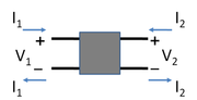
Figure 1: Example two-port network with symbol definitions. Notice the
port condition is satisfied: the same current flows into each port as leaves that port.
A Two Port Network (or four-terminal network, or quadrapole) is an electrical circuit or device with two pairs of terminals. Two terminals constitute a port if they satisfy the essential requirement known as the port condition: the same current must enter and leave a port.[1][2]
Examples include small-signal models for transistors (such as the hybrid-pi model), filters and matching networks. The analysis of passive two-port networks is an outgrowth of reciprocity theorems first derived by Lorentz. See review by Jasper J. Goedbloed, Reciprocity and EMC measurements.
A two-port network makes possible the isolation of either a complete circuit or part of it and replacing it by its characteristic parameters. Once this is done, the isolated part of the circuit becomes a "black box" with a set of distinctive properties, enabling us to abstract away its specific physical buildup, thus simplifying analysis. Any linear circuit with four terminals can be transformed into a two-port network provided that it does not contain an independent source and satisfies the port conditions.
The parameters used in order to describe a two-port network are the following: z, y, h, g, T. They are usually expressed in matrix notation and they establish relations between the following parameters (see Figure 1):
 = Input voltage
 = Output voltage
 = Input current
 = Output current
These variables are most useful at low to moderate frequencies. At high frequencies (for example, microwave frequencies) power and energy are more useful variables, and the two-port approach based on current and voltages that is discussed here is replaced by an approach based upon scattering parameters.
Though some authors use the terms two-port network and four-terminal network interchangeably, the latter represents a more general concept. Not all four-terminal networks are two-port networks. A pair of terminals can be called a port only if the current entering one is equal to the current leaving the other (the port condition). Only those four-terminal networks in which the four terminals can be paired into two ports can be called two-ports.[1][2]
Impedance parameters (z-parameters)
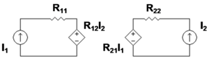
Figure 2: z-equivalent two port showing independent variables
I1 and
I2. Although resistors are shown, general impedances can be used instead.
- For more information, see: Impedance parameters.
![{\displaystyle \left[{\begin{array}{c}V_{1}\\V_{2}\end{array}}\right]=\left[{\begin{array}{cc}z_{11}&z_{12}\\z_{21}&z_{22}\end{array}}\right]\left[{\begin{array}{c}I_{1}\\I_{2}\end{array}}\right]}](https://wikimedia.org/api/rest_v1/media/math/render/svg/7645f82f97b057892f6d77d80bbf01b985aaae0f) .
.


Notice that all the z-parameters have dimensions of ohms.
Example: bipolar current mirror with emitter degeneration
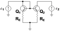
Figure 3: Bipolar current mirror:
i1 is the
reference current and
i2 is the
output current; lower case symbols indicate these are
total currents that include the DC components
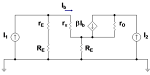
Figure 4: Small-signal bipolar current mirror:
I1 is the amplitude of the small-signal
reference current and
I2 is the amplitude of the small-signal
output currentFigure 3 shows a bipolar current mirror with emitter resistors to increase its output resistance.[3] Transistor Q1 is diode connected, which is to say its collector-base voltage is zero. Figure 4 shows the small-signal circuit equivalent to Figure 3. Transistor Q1 is represented by its emitter resistance rE ≈ VT / IE (VT = thermal voltage, IE = Q-point emitter current), a simplification made possible because the dependent current source in the hybrid-pi model for Q1 draws the same current as a resistor 1 / gm connected across rπ. The second transistor Q2 is represented by its hybrid-pi model. Table 1 below shows the z-parameter expressions that make the z-equivalent circuit of Figure 2 electrically equivalent to the small-signal circuit of Figure 4.
| Table 1 |
Expression |
Approximation
|

|
 
|
 
|

|
  
|

|

|
     
|

|

|
|
|
The negative feedback introduced by resistors RE can be seen in these parameters. For example, when used as an active load in a differential amplifier, I1 ≈ -I2, making the output impedance of the mirror approximately R22 -R21 ≈ 2 β rORE /( rπ+2RE ) compared to only rO without feedback (that is with RE = 0 Ω) . At the same time, the impedance on the reference side of the mirror is approximately R11 -R12 ≈  , only a moderate value, but still larger than rE with no feedback. In the differential amplifier application, a large output resistance increases the difference-mode gain, a good thing, and a small mirror input resistance is desirable to avoid Miller effect.
Admittance parameters (y-parameters)
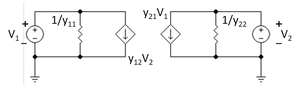
Figure 5: Y-equivalent two port showing independent variables
V1 and
V2. Although resistors are shown, general admittances can be used instead.
- For more information, see: Admittance parameters.
![{\displaystyle \left[{\begin{array}{c}I_{1}\\I_{2}\end{array}}\right]=\left[{\begin{array}{cc}y_{11}&y_{12}\\y_{21}&y_{22}\end{array}}\right]\left[{\begin{array}{c}V_{1}\\V_{2}\end{array}}\right]}](https://wikimedia.org/api/rest_v1/media/math/render/svg/1f0a34623af2771a0510c92e6a21ac4e6de760aa) .
.
where


The network is said to be reciprocal if  . Notice that all the Y-parameters have dimensions of siemens.
Hybrid parameters (h-parameters)
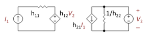
Figure 6: H-equivalent two-port showing independent variables
I1 and
V2;
h22 is reciprocated to make a resistor
 .
.
where


Often this circuit is selected when a current amplifier is wanted at the output. The resistors shown in the diagram can be general impedances instead.
Notice that off-diagonal h-parameters are dimensionless, while diagonal members have dimensions the reciprocal of one another.
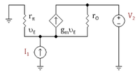
Figure 7: Common-base amplifier with AC current source
I1 as signal input and unspecified load supporting voltage
V2 and a dependent current
I2.
Note: Tabulated formulas in Table 2 make the h-equivalent circuit of the transistor from Figure 6 agree with its small-signal low-frequency hybrid-pi model in Figure 7. Notation: rπ = base resistance of transistor, rO = output resistance, and gm = transconductance. The negative sign for h21 reflects the convention that I1, I2 are positive when directed into the two-port. A non-zero value for h12 means the output voltage affects the input voltage, that is, this amplifier is bilateral. If h12 = 0, the amplifier is unilateral.
| Table 2 |
Expression |
Approximation
|

|

|

|

|

|

|

|

|

|

|

|
 << 1 << 1
|
Inverse hybrid parameters (g-parameters)
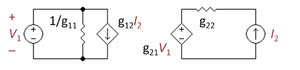
Figure 8: G-equivalent two-port showing independent variables
V1 and
I2;
g11 is reciprocated to make a resistor
 .
.
where


Often this circuit is selected when a voltage amplifier is wanted at the output. Notice that off-diagonal g-parameters are dimensionless, while diagonal members have dimensions the reciprocal of one another. The resistors shown in the diagram can be general impedances instead.
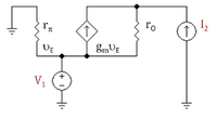
Figure 9: Common-base amplifier with AC voltage source
V1 as signal input and unspecified load delivering current
I2 at a dependent voltage
V2.
Note: Tabulated formulas in Table 3 make the g-equivalent circuit of the transistor from Figure 8 agree with its small-signal low-frequency hybrid-pi model in Figure 9. Notation: rπ = base resistance of transistor, rO = output resistance, and gm = transconductance. The negative sign for g12 reflects the convention that I1, I2 are positive when directed into the two-port. A non-zero value for g12 means the output current affects the input current, that is, this amplifier is bilateral. If g12 = 0, the amplifier is unilateral.
| Table 3 |
Expression
|

|

|

|

|

|
|

|

|
ABCD-parameters
The ABCD-parameters are known variously as chain, cascade, or transmission parameters.[4]
 .
.
where


Note that we have inserted negative signs in front of the fractions in the definitions of parameters B and D. The reason for adpoting this convention (as opposed to the convention adopted above for the other sets of parameters) is that it allows us to represent the transmission matrix of cascades of two or more two-port networks as simple matrix multiplications of the matrices of the individual networks. This convention is equivalent to reversing the direction of I2 so that it points in the same direction as the input current to the next stage in the cascaded network.
This technique is exactly analogous to the use of ABCD matrices for ray tracing in the science of optics. See also ray transfer matrix.
Table of transmission parameters
The table below lists transmission parameters for some simple network elements.
| Element
|
Matrix
|
Remarks
|
| Series resistor
|

|
R = resistance
|
| Shunt resistor
|

|
R = resistance
|
| Series conductor
|

|
G = conductance
|
| Shunt conductor
|

|
G = conductance
|
| Series inductor
|

|
L = inductance
s = complex angular frequency
|
| Shunt capacitor
|

|
C = capacitance
s = complex angular frequency
|
Combinations of two-port networks
Series connection of two 2-port networks: Z = Z1 + Z2
Parallel connection of two 2-port networks: Y = Y1 + Y2
Example: Cascading two networks
Suppose we have a two-port network consisting of a series resistor R followed by a shunt capacitor C. We can model the entire network as a cascade of two simpler networks:


The transmission matrix for the entire network T is simply the matrix multiplication of the transmission matrices for the two network elements:


Thus:

Notes regarding definition of transmission parameters
1) It should be noted that all these examples are specific to the definition of transmission parameters given here. Other definitions exist in the literature, such as:

2) The format used above for cascading (ABCD) examples cause the "components" to be used backwards compared to standard electronics schematic conventions. This can be fixed by taking the transpose of the above formulas, or by making the  the left hand side (dependent variables). Another advantage of the form is that the output can be terminated (via a transfer matrix representation of the load) and then
  can be set to zero; allowing the voltage transfer function, 1/A to be read directly.
3) In all cases the ABCD matrix terms and current definitions should allow cascading.
4
Networks with more than 2 ports
While two port networks are very common (e.g. amplifiers and filters), other electrical networks such as directional couplers and isolators have more than 2 ports. The following representations can be extended to networks with an arbitrary number of ports:
They are extended by adding appropriate terms to the matrix representing the other ports. So 3 port impedance parameters result in the following relationship:
![{\displaystyle \left[{\begin{array}{c}V_{1}\\V_{2}\\V_{3}\end{array}}\right]=\left[{\begin{array}{ccc}Z_{11}&Z_{12}&Z_{13}\\Z_{21}&Z_{22}&Z_{23}\\Z_{31}&Z_{32}&Z_{33}\end{array}}\right]\left[{\begin{array}{c}I_{1}\\I_{2}\\I_{3}\end{array}}\right]}](https://wikimedia.org/api/rest_v1/media/math/render/svg/6f8103856d09b829a923cf5cf08e6269aae1139a) .
.
It should be noted that the following representations cannot be extended to more than two ports:
- Hybrid (h) parameters
- Inverse hybrid (g) parameters
- Transmission (ABCD) parameters
- Scattering Transmission (T) parameters
- ↑ 1.0 1.1
P.R. Gray, P.J. Hurst, S.H. Lewis, and R.G. Meyer (2001). Analysis and Design of Analog Integrated Circuits, Fourth Edition. New York: Wiley, §3.2, p. 172. ISBN 0471321680.
- ↑ 2.0 2.1
R. C. Jaeger and T. N. Blalock (2006). Microelectronic Circuit Design, Third Edition. Boston: McGraw-Hill, §10.5 §13.5 §13.8. ISBN 9780073191638.
- ↑ The emitter-leg resistors counteract any current increase by decreasing the transistor VBE. That is, the resistors RE cause negative feedback that opposes change in current. In particular, any change in output voltage results in less change in current than without this feedback, which means the output resistance of the mirror has increased.
- ↑ David M. Pozar (2005). Microwave Engineering, 3rd Edition. John Wiley & Sons, Chapter 4: pp. 161-221. ISBN 047164451X (Softcover).


